Building semiconducting nanostructures on graphene – for making novel flexible electronics and optoelectronics devices – is no easy task because graphene is unreactive thanks to its inert sp2-hybridized carbon-carbon bonds. Researchers at the Massachusetts Institute of Technology may now have found a way of overcoming this problem by growing semiconducting zinc oxide nanowire arrays on graphene using a process that modifies the surface of the carbon material while preserving its unique electronic properties.
Schematic of the device
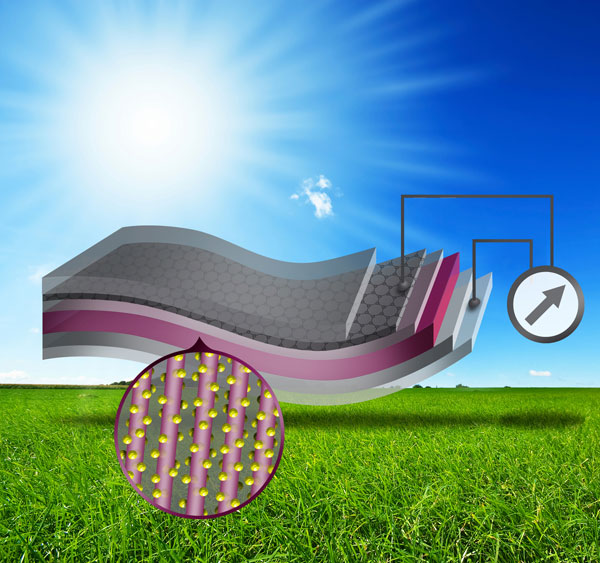
A team led by Silvija Gradecak has succeeded in growing ZnO nanowire arrays on graphene by modifying the surface of the carbon material with conducting polymer interlayers. The researchers synthesized ZnO seed layers on the interfacial polymer layers, which results in well ordered ZnO nanowire growth via a low-temperature hydrothermal process. "The polymer coating process, the ZnO seed layer deposition and hydrothermal ZnO nanowire growth are all possible in solution and under ambient conditions," explained Gradecak. "What is more, the interfacial conductive polymer coating allows for efficient charge transfer between the ZnO nanowires and graphene, so preserving the unique electronic properties of the latter."
Solar cells from the hybrid structure
As a case in point, the MIT team then used their ZnO nanowire-graphene hybrid structure to make cathode-based solar cells using two different photoactive materials: PbS quantum dots and the conjugated polymer P3HT. The devices had power conversion efficiencies of 4.2% and 0.5%, respectively.
"In the case of ZnO nanowire/P3HT hybrid solar cells, we spin coated a solution of P3HT on the ZnO nanowire arrays," said Gradecak. "The substrate was then annealed to ensure that the maximum amount of P3HT infiltrated into the voids of the nanowire arrays. We then thermally evaporated the top gold anode."
One big advantage of using ZnO nanowires is that the spacing between the wires is compatible with the diffusion length of excitons (electrons and holes) in conjugated polymers like P3HT, which is around 20 nm. Charges can thus be efficiently extracted in the device structure via one-dimensional charge transport pathways and thanks to the large interfacial area in the well ordered ZnO nanowire/P3HT heterojunction.
The ZnO nanowire/PBS quantum dots hybrid solar cells were made a little differently. Here, colloidal PbS quantum dots were infiltrated into the ZnO nanowire arrays by sequential layer-by-layer spin coating. The band gap in these devices can be tuned by controlling the composition and size of the quantum dots to maximize the range of solar spectrum light wavelengths that can be absorbed by the device.
"Our simple method for fabricating semiconducting nanostructures on graphene via interface engineering preserves graphene structural and electrical properties and hence could be applied to make a variety of nanoelectronic devices, such as light-emitting diodes," Gradecak told nanotechweb.org.
The team says that it is now busy investigating other graphene electrode-based and solution processable flexible photovoltaic systems with a view to making devices that are as good or better than their conventional counterparts.
The current work is detailed in Nano Letters.