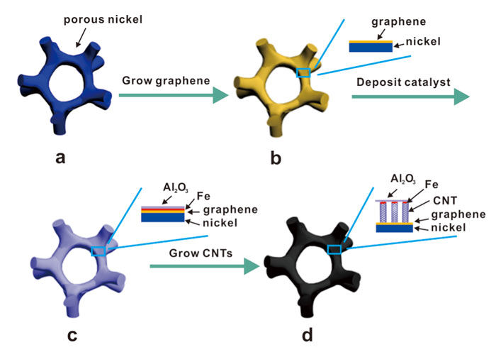
Making metal-graphene-CNTs.
Graphene and carbon nanotubes have many excellent electronic and mechanical properties, such as high carrier mobility, high electrical and thermal conductivity, exceptional tensile strength and large surface area. Combining the 2D graphene with the 1D nanotubes allows these characteristics to be exploited in 3D and so benefit energy storage and nanoelectronic technologies. However, it is difficult to covalently fuse the two materials together because they are grown on different substrates – alumina and iron for CNTs and metal catalysts (like nickel and copper) for graphene. Indeed, previous attempts to do so have resulted in CNTs that were physisorbed on the graphene plane rather than joined up to it by covalent sp2carbon-sp2 carbon bonds.
James Tour and colleagues may now have found a way around this problem. The researchers used methane as the carbon source to grow few-layered graphene on porous nickel via chemical vapour deposition at 1000 °C. They then grew CNTs from this graphene using e-beam deposited Fe/Al2O3. The length of the CNT forests could be controlled by simply adjusting the growth time.
In this method, the iron catalysts play a key role because they etch graphene and catalyse the growth of the CNTs at the same time, explains Tour. The result is a metal-graphene-CNT hybrid that can directly be used to make field-emitter devices and double-layer capacitors that are just as good, or better, than the best supercapacitors and field-emitters on the market today, he says.
Best properties
“For field-emitter devices, the turn-on field, measured at a current density of 0.01 mA/cm2, is just 0.26 V/um, which is one the lowest values ever reported (and a low value is desired here),” he told nanotechweb.org. “For the same device, the current density at a field of 0.87 V/um is 12.67 mA/cm2, which is one of the highest reported values to date (the higher the current density the better).”
For double-layer capacitors, the specific capacitance is around 100 F/g, a figure that compares well with the best reported values of such devices made with carbon-based materials, he adds.
High-resolution aberration-corrected transmission electron microscopy studies on the hybrid revealed that the graphene and CNTs were covalently bound together, something that ensures the seamless junction between the two materials.
The Rice researchers would now like to introduce additives, such as nitrogen, into the graphene and CNTs during the growth process. “The resulting doped hybrid materials could have potential applications in fuel cells and lithium batteries,” said Tour.
The current work is detailed in ACS Nano.