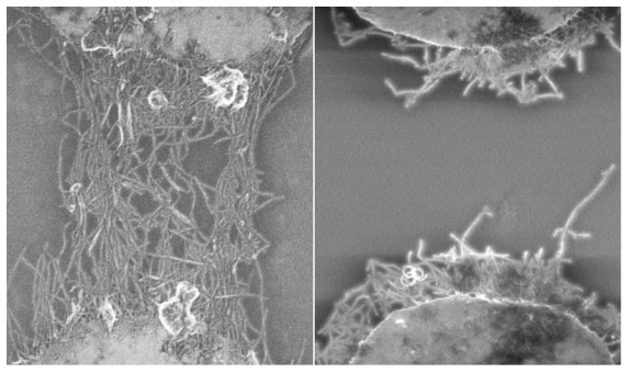
Researchers from the Department of Electrical and Computer Engineering at the University of British Columbia in Canada are studying the interplay between the two forces in various solutions. To obtain solutions that can be used for a fair comparison, the team took a creative approach and prepared one type of solution from the other.
The scientists then performed a series of systematic experiments and simulations, which showed that for different solutions the strength of the forces change drastically and, therefore, the fabricated devices look very different. They observed that the direction and effectiveness of the electrothermal force is orders of magnitude different in the various solutions, which could lead to inconsistent and irreproducible results if ignored during production.
Engineering considerations
The drastic differences among the nanotube patterns deposited from various solutions highlights the importance of engineering the solution properties to generate the desired device structure.
When depositing material from a surfactant-containing solution, the CNTs tend to cover the edges of metallic electrodes, which makes this approach more suitable for applications involving dense nanotube patterns. On the other hand, avoiding surfactants and, instead, functionalizing the nanotubes to disperse them in the solution might be more appropriate for making electronic and photonic devices because in this case the CNTs bridge the electrodes more effectively.
About the author
Ali Kashefian Naieni is a PhD candidate in the Electrical and Computer Engineering Department at the University of British Columbia. His research focuses on simulation, fabrication and characterization of nanomaterial-based devices from solutions. Alireza Nojeh received his BS and MS degrees in electrical engineering from Sharif University of Technology, Tehran, Iran. His work there focused on optoelectronic modulators based on interface charge layers. He went on to receive a DEA degree in electronics/optoelectronics from the University of Paris XI, Orsay, France, where he worked on high-electron mobility transistors, and a PhD degree in electrical engineering from Stanford University, Stanford, California, US (2006). At Stanford, he worked on carbon nanotubes, focusing on nanoscale electron emitters. He then joined the University of British Columbia, where he is currently an associate professor of electrical and computer engineering. His research interests are still in nanotechnology, in particular in carbon nanotube devices, interaction of light with nanostructures, electron sources, vacuum electronics and electron microscopy, solid-state electronics, micro/nanofabrication, and modeling and simulation of nanoscale structures.

